
The purpose of an inverter is to transform a DC waveform voltage into an AC signal in order to inject power into a load (e.g. the power grid) at a given frequency and with a small phase angle (φ ≈ 0). A simplified circuit for a single phase unipolar Pulse-Width Modulation (PWM) is shown in Figure 2 (the same general scheme can be extended to a three phase system). In this schematic, a PV system, acting as a DC voltage source with some source inductance, is shaped into an AC signal through four IGBT switches in parallel with freewheeling diodes. These switches are controlled at the gate through a PWM signal, which is typically the output of an IC that compares a carrier wave (usually a sine wave of the desired output frequency) and a reference wave at a significantly higher frequency (typically a triangle wave at 5-20kHz). The output of the IGBTs is shaped into an AC signal suitable for use or grid injection through the application of various topologies of LC filters.
Inverters belong to a large group of static converters, which include many of today’s devices able to “convert” electrical parameters in input, such as voltage and frequency, so as to produce an output that is compatible with the requirements of the load.
Generally speaking, inverters are the devices capable of converting direct current into alternating current and are quite common in industrial automation applications and electric drives. The architecture and the design of different inverter types changes according to each specific application, even if the core of their main purpose is the same (DC to AC conversion).
1.Standalone and Grid-Connected Inverters
Inverters used in photovoltaic applications are historically divided into two main categories:
: Standalone inverters
: Grid-connected inverters
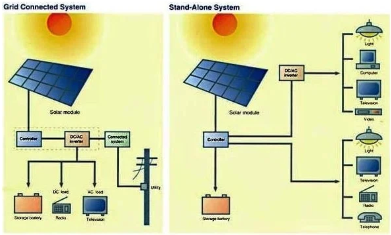
Standalone inverters are for the applications where the PV plant is not connected to the main energy distribution network. The inverter is able to supply electrical energy to the connected loads, ensuring the stability of the main electrical parameters (voltage and frequency). This keeps them within predefined limits, able to withstand temporary overloading situations. In this situation, the inverter is coupled with a battery storage system in order to ensure a consistent energy supply.
Grid-connected inverters, on the other hand, are able to synchronize with the electrical grid to which they are connected because, in this case, voltage and frequency are “imposed” by the main grid. These inverters must be able to disconnect if the main grid fails in order to avoid any possible reverse supply of the main grid, which could represent a serious danger.
- Figure 1 - Example of Standalone system and Grid-connected system. Image courtesy of Biblus.
2.What is the Role of the Bus Capacitor
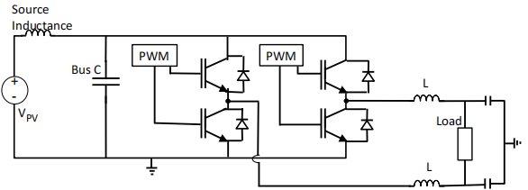
Figure 2: Pulsed Width Modulation (PWM) single-phase inverter setup. The IGBT switches, along with LC output filter, shape the DC input signal into a usable AC signal. This induces a deleterious voltage ripple across the PV terminals. The bus capacitor is sized in order to reduce this ripple.
The operation of the IGBTs introduces a ripple voltage onto the terminal of the PV array. This ripple is deleterious to the operation of the PV system, since the nominal voltage applied to the terminals should be held at the max power point (MPP) of the IV curve in order to extract the most power. A voltage ripple on the PV terminals will oscillate the power extracted from the system , resulting in
a lower average power output (Figure 3). A capacitor is added onto the bus in order to smooth out the voltage ripple.
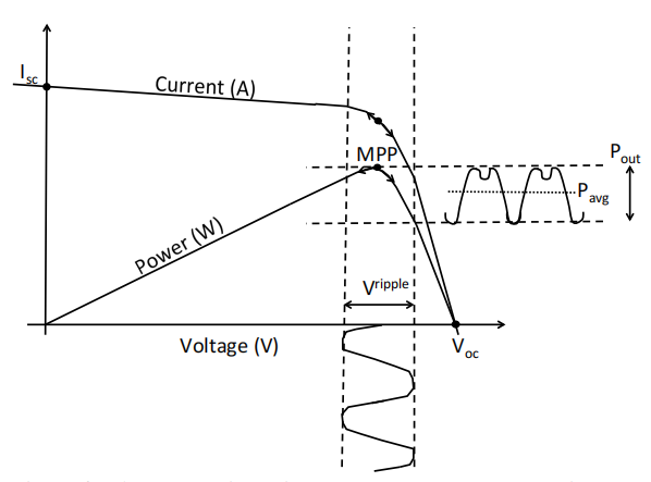
Figure 3: A voltage ripple introduced onto the PV terminals by the PWM inverter scheme shifts the applied voltage off the max power point (MPP) of the PV array. This introduces a ripple in the power output of the array so that the average output power is lower than the nominal MPP
The amplitude (peak to peak) of the voltage ripple is determined by the switching frequency, PV voltage, bus capacitance, and filter inductance according to:
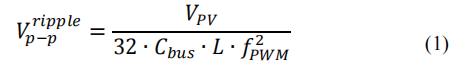
where:
VPV is the solar panel DC voltage,
Cbus is the capacitance of the bus capacitor,
L is the inductance of the filter inductors,
fPWM is the switching frequency.
Equation (1) applies to an ideal capacitor that prevents charge from flowing through the capacitor during charging and then discharges the energy located in the electric field with no resistance. In reality, no capacitor is ideal (Figure 4) but is composed of multiple elements. In addition to the ideal capacitance, the dielectric is not perfectly resistive and a small leakage current flows from the anode to cathode along a finite shunt resistance (Rsh), bypassing the dielectric capacitance (C). When current through the capacitor is flowing, the pins, foils, and dielectric are not perfectly conducting and there is an equivalent series resistance (ESR) in series with the capacitance. Finally, the capacitor does store some energy in the magnetic field, so there is an equivalent series inductance (ESL) in series with the capacitance and ESR.
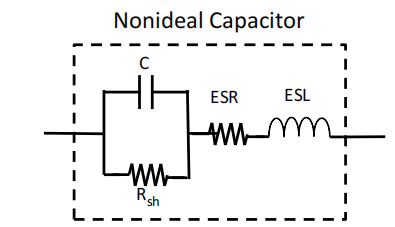
Figure 4: Equivalent circuit of a generic capacitor. A capacitor is composed of many non-ideal elements, including dielectric capacitance (C), a non-infinite shunt resistance through the dielectric that bypasses the capacitor, series resistance (ESR), and series inductance (ESL).
Even in a component as seemingly simple as a capacitor, there exist multiple elements that can fail or degrade. Each of these elements can affect the behavior of the inverter, both on the AC and DC sides. In order to determine the effect degradation of non-ideal capacitor components has on the voltage ripple introduced across the PV terminals, a PWM unipolar H-bridge inverter (Figure 2) was simulated using SPICE. The filter capacitors and inductors are held at 250µF and 20mH, respectively. The SPICE models for the IGBTs are derived from the work of Petrie et al.The PWM signal, which controls the IGBT switches, is determined by a comparator and inverting comparator circuit for the high and low-side IGBT switches, respectively. The input for the PWM controls are a 9.5V, 60Hz sine carrier wave and a 10V, 10kHz triangular wave.
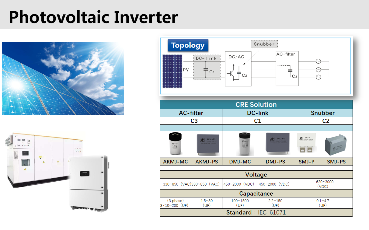
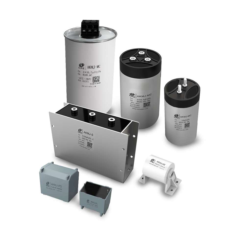
- CRE solution
CRE is a high-tech enterprise speciallizing in the production of film capacitors,focusing on application of power electrionics.
CRE offer the mature solution of film capacitor series for PV inverter which including DC-link, AC-filter and snubber.
Post time: Dec-01-2023